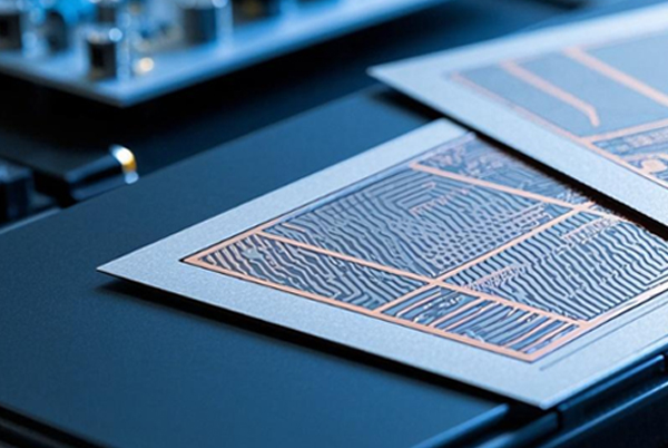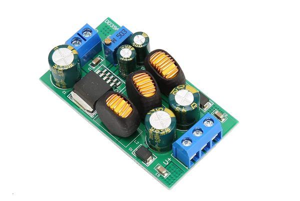
PCB Layout Design
This comprehensive guide walks through the entire PCB layout workflow—from schematics to final checks—detailing best practices for grid settings, component placement, special part handling, routing approaches, and verification methods. It also provides actionable solutions to five frequent design challenges, offering value to both novices and experienced designers seeking to elevate their PCB quality.