TOPFAST PCB One-Stop Solutions

Blog

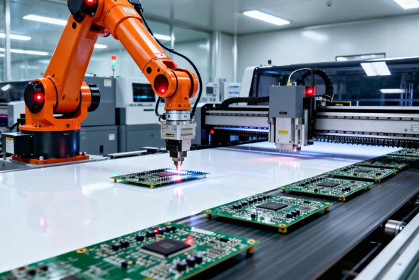
PCB and IoT

The critical role of printed circuit boards in IoT devices encompasses signal transmission, power management, and structural integration. This analysis explores how advanced technologies such as HDI and SiP address the challenges of miniaturization and low power consumption in IoT devices.
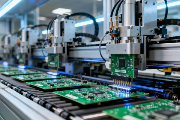

PCB Automated Assembly

Comparison of Manual and Automated PCB Assembly

Comprehensively compare the technical characteristics, application scenarios, and economic benefits of manual assembly versus automated assembly. Conduct a detailed analysis of differences between the two assembly methods in terms of placement accuracy, soldering quality, environmental control, and cost composition. Provide decision-making guidelines tailored to varying production volumes and complexity levels, offering practical reference for electronics manufacturers to optimize production processes and enhance product quality.

High-Speed PCB Design

Key PCB Design Strategies and Modern Manufacturing Techniques

Delve into core strategies such as layered design, component placement, routing rules, and power management. Explore advanced techniques including high-speed signal processing, thermal optimization, and design for manufacturability. Through practical case studies and insights, this guide systematically enhances readers’ PCB design capabilities to achieve efficient and stable electronic products.

ai and pcb

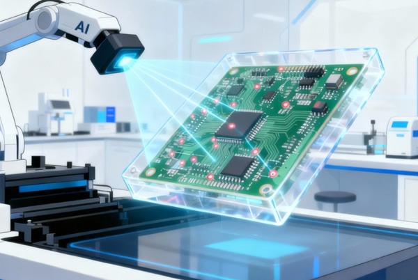
Applications of AI in PCB Design

Current Applications and Future Trends of Artificial Intelligence in PCB Design AI will be deeply integrated into the entire PCB design process through generative design, reinforcement learning, and cloud-native platforms. Simultaneously, it offers solutions to challenges such as data quality and adaptation to complex scenarios, providing a forward-looking perspective for the industry’s transition toward intelligent design.

Thin-film ceramic PCB

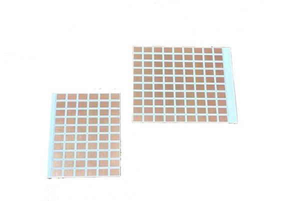
Thin-Film Ceramic Circuit Boards

Thin-film ceramic circuit boards represent high-end products in the electronic packaging field. Utilizing semiconductor microfabrication techniques such as sputtering, photolithography, and electroplating, they create precision circuits with line widths down to the micrometer level on ceramic substrates. Compared to thick-film technology, they offer higher wiring density, superior high-frequency performance, and enhanced reliability. These boards are widely used in demanding applications such as 5G communications, microwave components, and high-power lasers, where precision and thermal management are critical.

1 30 31 32 56