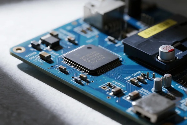
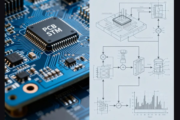
TOPFAST PCB One-Stop Solutions

Blog

PCB Assembly FAQs

PCB Assembly FAQs(Frequently Asked Questions)

Common issues encountered during the PCB assembly process, including document requirements, component specifications, panel design, process standards, and testing services, are addressed to help customers efficiently prepare orders and ensure high-quality production outcomes. As a professional PCBA service provider, Topfast offers transparent pricing, flexible order options, and end-to-end support, catering to a wide range of needs from R&D prototyping to mass production.

PCB OSP process

PCB OSP Surface Treatment Process

The technical characteristics, process flow, and quality control of PCB OSP surface treatment are discussed, and the performance differences between mainstream processes such as HASL, ENIG, silver immersion, and tin immersion are comprehensively compared. Topfast provides a practical surface treatment selection guide to help optimize product design and manufacturing processes.

ENIG process

ENIG (Electroless Nickel Immersion Gold) Process

The ENIG (electroless nickel immersion gold) process is crucial for PCB surface treatment. It offers excellent solderability and corrosion resistance. Topfast provides reliable ENIG PCB manufacturing services. With our extensive experience and strict quality control, we ensure that our products meet high-quality standards.

HASL process

PCB HASL and Lead-Free HASL Processes

HASL hot air leveling process, including the alloy composition, process flow, and performance differences between leaded and lead-free HASL. A detailed analysis of the characteristics and application scenarios of ENIG electroplating and OSP anti-oxidation processes. As a professional PCB manufacturer, Topfast possesses comprehensive surface treatment process capabilities and a robust quality control system, enabling us to provide optimal surface treatment solutions for various electronic products.

4-Layer PCB

4-layer 1.6 mm PCB laminate structure

The laminate structure of a 4-layer 1.6 mm PCB is analyzed, focusing on the advantages of this standard thickness PCB in terms of impedance control, signal integrity, and EMC. At the same time, the application scenarios of 4-layer boards of different thicknesses are compared, and professional manufacturing process analysis is provided.

8-Layer PCB

8-Layer PCB

8-layer PCB precision lamination design, signal integrity optimization, advanced material application, and manufacturing processes. As well as a complete reliability verification system and technical support services. Topfast PCB provides professional 8-layer PCB solutions.

1 32 33 34 49