Table of Contents
Engineering Review for Complex PCB Projects
TOPFAST provides engineering evaluation and manufacturing support for advanced PCB projects that require specialized materials, complex structures, and stringent performance requirements.
Whether your project involves HDI PCB, High-Speed PCB, High-Frequency PCB, Rigid-Flex PCB, Heavy Copper PCB, or high-layer count designs, our engineering team can review your requirements and provide professional manufacturing recommendations.
Submit your design files and project specifications through the inquiry form to receive a technical assessment and manufacturing feasibility review.
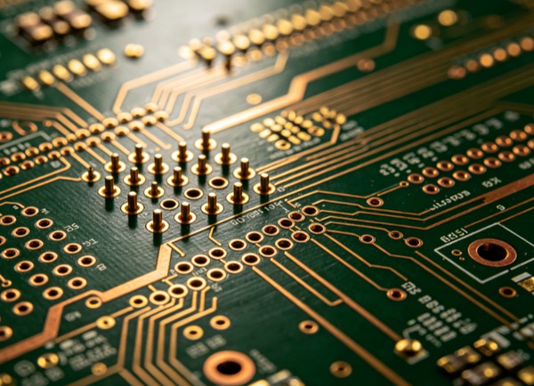
Advanced PCB Technologies We Support
Advanced electronic products often require PCB technologies beyond standard multilayer boards. TOPFAST supports a wide range of advanced PCB solutions for demanding applications.
HDI PCB
High-Density Interconnect (HDI) technology enables higher routing density and compact product designs.
Capabilities include:
- Laser Microvias
- Blind Vias
- Buried Vias
- Sequential Lamination
- Fine Line Technology
Applications:
- Consumer Electronics
- Medical Devices
- Industrial Controllers
- Portable Devices
High-Speed PCB
High-speed digital systems require precise impedance control and optimized signal routing.
Capabilities include:
- Controlled Impedance
- Differential Pair Routing
- Back Drilling
- Low-Loss Materials
- Signal Integrity Optimization
Applications:
- Data Centers
- Servers
- Networking Equipment
- AI Computing Systems
High-Frequency PCB
RF and microwave applications require stable dielectric performance and low signal loss.
Supported materials include:
- Rogers
- Taconic
- Isola
- PTFE-Based Materials
Applications:
- 5G Infrastructure
- RF Modules
- Radar Systems
- Satellite Communication
Rigid-Flex PCB
Rigid-flex technology combines rigid and flexible circuits into a single structure.
Advantages:
- Reduced Connectors
- Improved Reliability
- Space Saving
- Simplified Assembly
Applications:
- Aerospace Electronics
- Medical Equipment
- Industrial Sensors
- Portable Devices
Heavy Copper PCB
Heavy copper PCB technology is designed for high-current and power applications.
Capabilities include:
- Up to 20oz Copper
- Enhanced Thermal Management
- High Current Capacity
- Improved Mechanical Strength
Applications:
- Power Supplies
- Solar Inverters
- Industrial Automation
- Motor Control Systems
High Layer Count PCB
Complex electronic systems often require multilayer PCB structures with demanding signal integrity requirements.
Capabilities include:
- 20+ Layer PCB
- 30+ Layer PCB
- Backplane PCB
- Hybrid Material Stackups
- Controlled Impedance Structures
Applications:
- Telecommunications
- Aerospace Systems
- Semiconductor Equipment
- Military Electronics
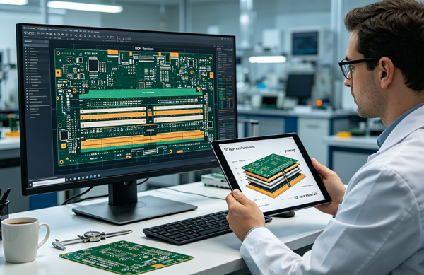
Engineering Review Process
Every advanced PCB inquiry is reviewed by experienced engineers before quotation and production planning.
[IMAGE: Engineer Reviewing PCB Cost Analysis]
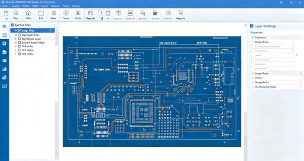
Step 1 – Submit Your Inquiry
Upload available design information, including:
- Gerber Files
- ODB++
- PCB Drawings
- Stackup Requirements
Step 2 – Technical Evaluation
Our engineering team reviews:
- PCB Structure
- Material Selection
- Manufacturing Feasibility
- Design Complexity
Step 3 – DFM Analysis
Design for Manufacturing (DFM) analysis helps identify potential risks before production.
Review items include:
- Trace Width
- Trace Spacing
- Via Structures
- Annular Rings
- Drill Sizes
- Registration Requirements
Step 4 – Engineering Feedback
Where appropriate, our engineers provide recommendations to improve manufacturability, reliability, and production efficiency.
Step 5 – Quotation and Lead Time Confirmation
After technical review, we provide:
- Manufacturing Assessment
- Recommended Processes
- Estimated Lead Time
- Commercial Quotation
Information Required for Evaluation
Providing complete project information helps accelerate the review process and improve quotation accuracy.
Design Files
Preferred formats include:
- Gerber Files
- ODB++
- IPC-2581
- PCB Drawings
- Stackup Documentation
Technical Specifications
Please provide:
- Layer Count
- Board Dimensions
- Material Requirements
- Board Thickness
- Copper Weight
- Surface Finish
- Impedance Requirements
Project Details
Additional information may include:
- Product Application
- Prototype Quantity
- Production Quantity
- Target Lead Time
- Special Reliability Requirements
Manufacturing Capabilities
TOPFAST supports both prototype and production manufacturing for advanced PCB projects.
Advanced PCB Capabilities
| Technology | Capability |
|---|---|
| HDI PCB | Supported |
| Blind Vias | Supported |
| Buried Vias | Supported |
| Microvias | Supported |
| High Frequency Materials | Supported |
| Controlled Impedance | Supported |
| Heavy Copper PCB | Supported |
| Rigid-Flex PCB | Supported |
| High Layer Count PCB | Supported |
| Back Drilling | Supported |
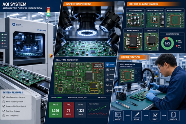
Quality Assurance
Advanced PCB manufacturing requires strict quality control throughout the production process.
Our inspection capabilities include:
- Automated Optical Inspection (AOI)
- X-Ray Inspection
- Flying Probe Testing
- Impedance Testing
- Cross-Section Analysis
- Electrical Testing
Industries We Serve
Advanced PCB technologies are widely used in industries where reliability and performance are critical.
Applications include:
Telecommunications
- 5G Infrastructure
- Network Equipment
- Data Transmission Systems
Industrial Electronics
- Automation Systems
- Industrial Control Equipment
- Power Electronics
Medical Devices
- Diagnostic Equipment
- Monitoring Systems
- Portable Medical Devices
Aerospace and Defense
- Communication Systems
- Navigation Equipment
- High-Reliability Electronics
Automotive Electronics
- ADAS Systems
- EV Power Control
- Automotive Communication Modules
Why Choose TOPFAST for Advanced PCB Projects

Engineering Expertise
Our engineering team evaluates complex PCB requirements before production begins.
Advanced Manufacturing Support
We support advanced PCB technologies and specialized manufacturing processes.
DFM and Stackup Optimization
Engineering review helps reduce manufacturing risks and improve project success rates.
Prototype to Production
Support is available from early-stage development through volume manufacturing.
Fast Technical Response
Most advanced PCB inquiries receive an initial engineering review within one business day.
Submit Your Advanced PCB Inquiry
Complex PCB projects require more than standard manufacturing capabilities. Early engineering involvement helps identify challenges, improve manufacturability, and reduce project risk.
If your project involves HDI structures, RF materials, controlled impedance, rigid-flex designs, heavy copper requirements, or other advanced PCB technologies, submit your inquiry today.
Upload your files, share your technical requirements, and our engineering team will review your project and provide a professional manufacturing assessment.
Have a Complex PCB Project?
Upload Your Design Files
Receive Professional Engineering Review
Get Manufacturing Recommendations and Quotation Support