Comprehensive Analysis of Double-Layer PCBs: Structure and Applications
Table of Contents
What is a Double-Layer PCB?
Double-layer PCBs (double-sided printed circuit boards) serve as core components in modern electronics manufacturing, featuring an innovative structure with conductive layers arranged on both sides of the substrate. This design achieves a perfect balance between routing density and manufacturing costs by laminating copper onto both sides of an insulating base material (typically FR-4) and utilizing precision via technology for interlayer interconnections.
Technical Features and Performance Advantages
Structural Design Characteristics
- Dual-side layout: Components and traces can be arranged on both top and bottom layers
- Via interconnections: Mechanical drilling or laser drilling enables electrical connections between layers
- Dielectric layer: Epoxy glass cloth substrate provides stable dielectric performance
Performance Parameter Comparison
| Characteristic | Single-Layer PCB | Double-Layer PCB | Multi-Layer PCB (4-layer) |
|---|---|---|---|
| Wiring Density | Low (50-80 points/cm²) | Medium (100-150 points/cm²) | High (200-300 points/cm²) |
| Unit Cost (10×10cm) | $0.3-0.6 | $0.8-1.2 | $2.3-3.8 |
| Production Cycle (bulk) | 3 days | 4-5 days | 7-10 days |
| Maximum Frequency | Below 10MHz | Below 50MHz | Above 1GHz |
| Anti-interference Capability | Average | Good | Excellent |
In-Depth Analysis of Application Fields
Consumer Electronics
Wearable Devices: Smart wristbands utilize a double-layer PCB for compact layouts, with thickness controllable within 0.8mm
Audio Equipment: Bluetooth earphones and portable speakers achieve superior sound quality through optimized wiring design
Power Management: Power banks and chargers employ a double-layer design to balance heat dissipation and efficiency
Automotive Electronic Systems
Body Control Modules: Window control, seat adjustment systems widely use a double-layer PCB
Sensor Systems: Tire pressure monitoring, temperature sensors adopt a double-layer board design
Entertainment Systems: Ideal choice for car audio and central control display devices
Industrial Control Equipment
Automation Controllers: PLC control modules use a double-layer PCB to ensure stable operation
Measuring Instruments: Digital multimeters, oscilloscopes, and other test equipment
Power Equipment: Industrial power supplies and converters
Communication Equipment
Network Devices: Basic circuit boards for switches and routers
Wireless Modules: Carriers for WiFi and Bluetooth modules
Transmission Equipment: Fiber optic conversion and signal transmission devices
Design Considerations and Optimization Strategies
Electrical Performance Optimization
- Layering strategy: “Top signal + bottom power” design reduces interference
- Impedance control: Precise calculation of trace width and spacing ensures signal integrity
- Shielding design: Critical signal lines use ground shielding to reduce EMI interference
Mechanical Structure Design
- Stiffener layout: Structural reinforcement in stress concentration areas
- Thermal expansion matching: Material selection with matched CTE reduces thermal stress
- Mounting hole design: Optimized hole position and size improve mounting stability
Thermal Management Solutions
- Copper distribution: Optimized power layer copper layout improves heat dissipation
- Thermal vias: Thermal via arrays under heating components
- Surface treatment: Surface treatment processes with good thermal conductivity
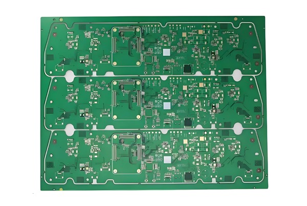
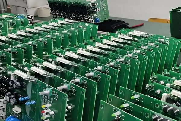
TOPFAST Double-Layer PCB Manufacturing Advantages
Precision Manufacturing Capabilities
TOPFAST utilizes advanced CNC equipment to ensure manufacturing precision:
- Dimensional accuracy: Outline machining accuracy reaches ±0.1mm
- Drilling precision: Minimum hole diameter 0.2mm, position accuracy ±0.05mm
- Line width accuracy: Minimum line width 0.1mm, tolerance controlled within ±10%
Quality Assurance System
- 100% electrical testing: Flying probe testing ensures electrical performance
- Environmental testing: Reliability verified through 1000 thermal cycle tests
- Impedance control: Strict control of interlayer dielectric thickness ensures signal integrity
Production Service Advantages
- Rapid response: 24-hour sample drawing, 72-hour prototyping
- Mass production: Standard delivery 4-5 days, expedited service 3 days
- Cost control: Reduced unit costs through scaled production
Technical Support Services
- Design review: Professional DFM analysis reports
- Process recommendations: Optimal process solutions based on product characteristics
- Problem resolution: Quick response to technical issues during production
Typical Application Cases
Smart Wristband Project
A renowned brand adopted TOPFAST’s double-layer PCB solution:
- Achieved ultra-thin design with 0.8mm board thickness
- Completed samples in 7 days, mass production in 15 days
- Product yield rate exceeded 99.8%
- Costs reduced by 40% compared to 4-layer board solutions
Industrial Controller Project
TOPFAST provided customized solutions for industrial clients:
- 2oz heavy copper design enhanced current carrying capacity
- Added thermal via design improved thermal performance
- Enhanced environmental adaptability through improved surface treatment
- Achieved 30% cost optimization in mass production
Conclusion and Outlook
Double-layer PCBs continue to play a vital role in electronics manufacturing, with their outstanding cost-performance ratio and moderate complexity securing an irreplaceable position across multiple industries. As material technology and manufacturing processes advance, the performance boundaries of double-layer PCBs are continually expanding.
Through continuous technological innovation and a comprehensive service system, TOPFAST delivers high-performance, highly reliable double-layer PCB solutions. From design support to volume manufacturing, and from process optimization to quality assurance, TOPFAST is committed to becoming the most trusted manufacturing partner for its customers.


Related Posts