Inside a PCB Factory: Step-by-Step Manufacturing Process
News
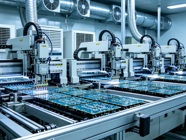
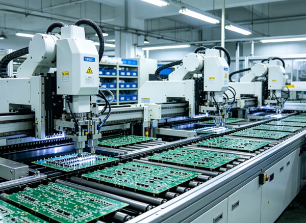
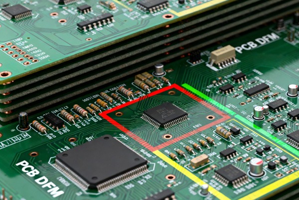
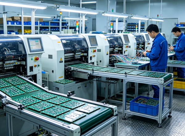
PCB Factory
Understanding how a PCB factory operates can help engineers and buyers make better sourcing decisions. This article takes you inside a PCB factory and explains the complete manufacturing process step by step, from raw materials to finished circuit boards. It covers key processes such as inner layer imaging, lamination, drilling, copper plating, and surface finishing. By understanding how PCBs are manufactured, you can improve design decisions, reduce production risks, and ensure higher product reliability.